- 您现在的位置:买卖IC网 > Sheet目录471 > MAX2044ETP+T (Maxim Integrated)IC MIXER UP/DOWN CONVER 20TQFN
�� �
�
�SiGe,� High-Linearity,� 2300MHz� to� 4000MHz�
�Upconversion/Downconversion� Mixer� with� LO� Buffer�
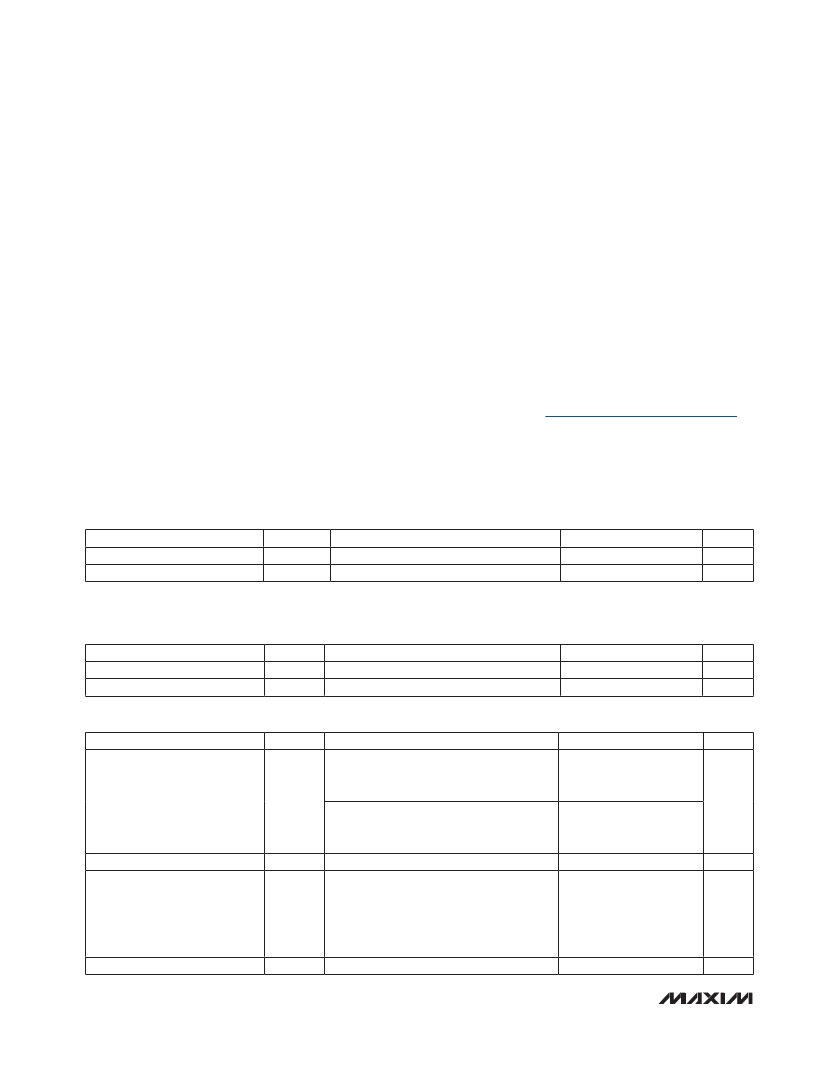
�ABSOLUTE� MAXIMUM� RATINGS�
�V� CC� to� GND..........................................................-0.3V� to� +5.5V�
�IF+,� IF-,� LOBIAS� to� GND� ..........................� -0.3V� to� (V� CC� +� 0.3V)�
�RF,� LO� Input� Power� .......................................................� +20dBm�
�RF,� LO� Current� (RF� and� LO� is� DC� shorted�
�to� GND� through� a� balun)...................................� .............50mA�
�Continuous� Power� Dissipation� (Note� 1)� .................................5W�
�B� JC� (Notes� 1,� 3)� ............................................................� +13� N� C/W�
�Operating� Case� Temperature�
�Range� (Note� 4)� .....................................� T� C� =� -40� N� C� to� +85� N� C�
�Junction� Temperature� .....................................................+150� N� C�
�Storage� Temperature� Range............................� -65� N� C� to� +150� N� C�
�Lead� Temperature� (soldering,� 10s)� ................................+300� N� C�
�B� JA� (Notes� 2,� 3)� ............................................................� +38� N� C/W�
�Note� 1:� Based� on� junction� temperature� T� J� =� T� C� +� (� B� JC� x� V� CC� x� I� CC� ).� This� formula� can� be� used� when� the� temperature� of� the�
�exposed� pad� is� known� while� the� device� is� soldered� down� to� a� PCB.� See� the� Applications� Information� section� for� details.�
�The� junction� temperature� must� not� exceed� +150� N� C.�
�Note� 2:� Junction� temperature� T� J� =� T� A� +� (� B� JA� x� V� CC� x� I� CC� ).� This� formula� can� be� used� when� the� ambient� temperature� of� the� PCB� is�
�known.� The� junction� temperature� must� not� exceed� +150� N� C.�
�Note� 3:� Package� thermal� resistances� were� obtained� using� the� method� described� in� JEDEC� specification� JESD51-7,� using� a� four-�
�layer� board.� For� detailed� information� on� package� thermal� considerations,� refer� to� www.maxim-ic.com/thermal-tutorial� .�
�Note� 4:� T� C� is� the� temperature� on� the� exposed� pad� of� the� package.� T� A� is� the� ambient� temperature� of� the� device� and� PCB.�
�Stresses� beyond� those� listed� under� “Absolute� Maximum� Ratings”� may� cause� permanent� damage� to� the� device.� These� are� stress� ratings� only,� and� functional�
�operation� of� the� device� at� these� or� any� other� conditions� beyond� those� indicated� in� the� operational� sections� of� the� specifications� is� not� implied.� Exposure� to� absolute�
�maximum� rating� conditions� for� extended� periods� may� affect� device� reliability.�
�5.0V� SUPPLY� DC� ELECTRICAL� CHARACTERISTICS�
�(Typical� Application� Circuit� ,� V� CC� =� 4.75V� to� 5.25V,� no� input� RF� or� LO� signals.� T� C� =� -40� N� C� to� +85� N� C,� unless� otherwise� noted.� Typical�
�values are at V� CC� = 5.0V, T� C� = +2� 5� N� C,� all� parameters� are� production� tested.)�
�PARAMETER�
�Supply� Voltage�
�Supply� Current�
�SYMBOL�
�V� CC�
�I� CC�
�CONDITIONS�
�MIN�
�4.75�
�TYP�
�5.0�
�138�
�MAX�
�5.25�
�155�
�UNITS�
�V�
�mA�
�3.3V� SUPPLY� DC� ELECTRICAL� CHARACTERISTICS�
�(Typical� Application� Circuit� ,� V� CC� =� 3.0V� to� 3.6V,� no� input� RF� or� LO� signals.� T� C� =� -40� N� C� to� +85� N� C,� unless� otherwise� noted.� Typical�
�values� are� at� V� CC� =� 3.3V,� T� C� =� +25� N� C,� parameters� are� guaranteed� by� design,� unless� otherwise� noted.)�
�PARAMETER�
�SYMBOL�
�CONDITIONS�
�MIN�
�TYP�
�MAX�
�UNITS�
�Supply� Voltage�
�Supply� Current�
�V� CC�
�I� CC�
�Total� supply� current,� V� CC� =� 3.3V�
�3.0�
�3.3�
�121�
�3.6�
�135�
�V�
�mA�
�RECOMMENDED� AC� OPERATING� CONDITIONS�
�PARAMETER�
�SYMBOL�
�CONDITIONS�
�MIN�
�TYP�
�MAX�
�UNITS�
�Typical� Application� Circuit� with� C1� =� 3.3nH�
�and� C12� =� 0.3pF,� see� Table� 1� for� details�
�2300�
�3000�
�RF� Frequency� Range�
�f� RF�
�(Note� 5)�
�Typical� Application� Circuit� with� C1� =� 8.2pF�
�and� C12� not� installed,� see� Table� 1� for�
�3000�
�4000�
�MHz�
�details� (Note� 5)�
�LO� Frequency�
�f� LO�
�(Note� 5)�
�2600�
�4300�
�MHz�
�Using� an� M/A-Com� MABAES0029� 1:1�
�transformer� as� defined� in� the� Typical�
�IF� Frequency�
�f� IF�
�Application� Circuit� ,� IF� matching�
�50�
�500�
�MHz�
�components� affect� the� IF� frequency� range�
�(Note� 5)�
�LO� Drive�
�P� LO�
�(Note� 5)�
�-3�
�0�
�+3�
�dBm�
�2�
�______________________________________________________________________________________�
�发布紧急采购,3分钟左右您将得到回复。
相关PDF资料
MAX2046ETJ+T
IC MULT HI GAIN VECTOR 32-TQFN
MAX2047EVKIT
EVAL KIT FOR MAX2047
MAX2051ETP+T
IC UP/DOWNCONVERSION MIXR 20TQFN
MAX2055EUP+TD
IC ADC DRVR/AMP VAR GAIN 20TSSOP
MAX2055EVKIT
EVAL KIT FOR MAX2055
MAX2056EVKIT
EVAL KIT FOR MAX2056
MAX2057EVKIT
EVAL KIT FOR MAX2057
MAX2058EVKIT
EVAL KIT FOR MAX2058
相关代理商/技术参数
MAX2044EVKIT#
功能描述:射频混合器 SiGe High-Linearity 2300MHz to 4000MHz Upconvervion/Downconversion Mixer w/LO Buffer RoHS:否 制造商:NXP Semiconductors 频率范围: 转换损失——最大: 工作电源电压:6 V 最大工作温度:+ 85 C 最小工作温度:- 40 C 安装风格:Through Hole 封装 / 箱体:PDIP-8 封装:Tube
MAX2044EVKIT+
功能描述:射频混合器 MAX2044 EVKIT RoHS:否 制造商:NXP Semiconductors 频率范围: 转换损失——最大: 工作电源电压:6 V 最大工作温度:+ 85 C 最小工作温度:- 40 C 安装风格:Through Hole 封装 / 箱体:PDIP-8 封装:Tube
MAX2045
制造商:MAXIM 制造商全称:Maxim Integrated Products 功能描述:High-Gain Vector Multipliers
MAX2045ETJ
功能描述:特殊用途放大器 High-Gain Vector Multiplier RoHS:否 制造商:Texas Instruments 通道数量:Single 共模抑制比(最小值): 输入补偿电压: 工作电源电压:3 V to 5.5 V 电源电流:5 mA 最大功率耗散: 最大工作温度:+ 70 C 最小工作温度:- 40 C 安装风格:SMD/SMT 封装 / 箱体:QFN-20 封装:Reel
MAX2045ETJ+
功能描述:特殊用途放大器 High-Gain Vector Multiplier RoHS:否 制造商:Texas Instruments 通道数量:Single 共模抑制比(最小值): 输入补偿电压: 工作电源电压:3 V to 5.5 V 电源电流:5 mA 最大功率耗散: 最大工作温度:+ 70 C 最小工作温度:- 40 C 安装风格:SMD/SMT 封装 / 箱体:QFN-20 封装:Reel
MAX2045ETJ+T
功能描述:特殊用途放大器 High-Gain Vector Multiplier RoHS:否 制造商:Texas Instruments 通道数量:Single 共模抑制比(最小值): 输入补偿电压: 工作电源电压:3 V to 5.5 V 电源电流:5 mA 最大功率耗散: 最大工作温度:+ 70 C 最小工作温度:- 40 C 安装风格:SMD/SMT 封装 / 箱体:QFN-20 封装:Reel
MAX2045ETJ-T
功能描述:特殊用途放大器 High-Gain Vector Multiplier RoHS:否 制造商:Texas Instruments 通道数量:Single 共模抑制比(最小值): 输入补偿电压: 工作电源电压:3 V to 5.5 V 电源电流:5 mA 最大功率耗散: 最大工作温度:+ 70 C 最小工作温度:- 40 C 安装风格:SMD/SMT 封装 / 箱体:QFN-20 封装:Reel
MAX2045EVKIT
功能描述:射频开发工具 RoHS:否 制造商:Taiyo Yuden 产品:Wireless Modules 类型:Wireless Audio 工具用于评估:WYSAAVDX7 频率: 工作电源电压:3.4 V to 5.5 V